(Hong Kong)

Product Summary
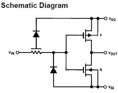
The CD4069UBCM is a Inverter Circuit. The device consists of six inverter circuits and is manufactured using complementary MOS (CMOS) to achieve wide power supply operating range, low power consumption, high noise immunity, and symmetric controlled rise and fall times. This device CD4069UBCM is intended for all general purpose inverter applications where the special characteristics of the MM74C901, MM74C907, and CD4049A Hex Inverter/Buffers are not required. In those applications requiring larger noise immunity the CD4069UBCM Hex Schmitt Trigger is suggested. All inputs are protected from damage due to static discharge by diode clamps to VDD and VSS.
Parametrics
CD4069UBCM absolute maximum ratings: (1)DC Supply Voltage (VDD): -0.5V to +18 VDC; (2)Input Voltage (VIN): -0.5V to VDD +0.5 VDC; (3)Storage Temperature Range (TS): -65 to +150℃; (4)Power Dissipation (PD): 700 mW; (5)Lead Temperature (TL) (Soldering, 10 seconds): 260℃.
Features
CD4069UBCM features: (1)Wide supply voltage range: 3.0V to 15V; (2)High noise immunity: 0.45 VDD typ.; (3)Low power TTL compatibility: Fan out of 2 driving 74L or 1 driving 74LS; (4)Equivalent to MM74C04.
Diagrams
| Image | Part No | Mfg | Description |  |
Pricing (USD) |
Quantity | ||||
|---|---|---|---|---|---|---|---|---|---|---|
 |
 CD4069UBCM |
Fairchild Semiconductor |
Inverters Inverter Circuits |
Data Sheet |
Negotiable |
|
||||
|
CD4069UBCM_Q |
Fairchild Semiconductor |
Inverters Inverter Circuits |
Data Sheet |
Negotiable |
|
||||
|
CD4069UBCMX |
Fairchild Semiconductor |
Inverters Inverter Circuits |
Data Sheet |
Negotiable |
|
||||