(Hong Kong)

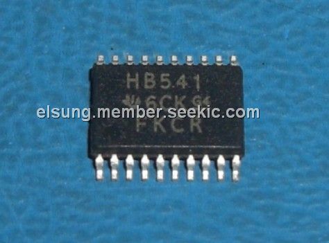
Product Summary
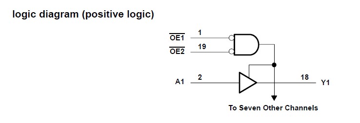
The HB541 octal buffer/driver is ideal for driving bus line or buffer memory address register. The HB541 features inputs and outputs on opposite sides of the package to facilitate printed circuit board layout. The 3-state control gate is a 2-input AND gate with active-low inputs so that if either output-enable (OE1 or OE2) input is high, all corresponding outputs are in the high-impedance state. The outputs of the HB541 provide noninverted data when they are not in the high-impedance state. To ensure the high-impedance state during power up or power down, OE should be tied to VCC through a pullup resistor; the minimum value of the resistor is determined by the current-sinking capability of the driver.
Parametrics
HB541 absolute maximum ratings: (1)Supply voltage range, VCC: –0.5 V to 7 V; (2)Input voltage range, VI: –0.5 V to 7 V; (3)Output voltage range, VO: –0.5 V to VCC + 0.5 V; (4)Input clamp current, IIK (VI < 0): –20 mA; (5)Output clamp current, IOK (VO < 0 or VO > VCC): ±20 mA; (6)Continuous output current, IO (VO = 0 to VCC): ±25 mA; (7)Continuous current through VCC or GND: ±75 mA.
Features
HB541 features: (1)Inputs Are TTL-Voltage Compatible; (2)Latch-Up Performance Exceeds 250 mA Per JESD 17; (3)ESD Protection Exceeds JESD 22.
Diagrams
 |
 HB54A1288KM |
Other |
|
Data Sheet |
Negotiable |
|
||||
|
HB54A2568FM |
Other |
|
Data Sheet |
Negotiable |
|
||||
|
HB54A2568KN-10B |
Other |
|
Data Sheet |
Negotiable |
|
||||
|
HB54A2568KN-A75B |
Other |
|
Data Sheet |
Negotiable |
|
||||
|
HB54A2568KN-B75B |
Other |
|
Data Sheet |
Negotiable |
|
||||
|
HB54A2569F1 |
Other |
|
Data Sheet |
Negotiable |
|
||||