(Hong Kong)

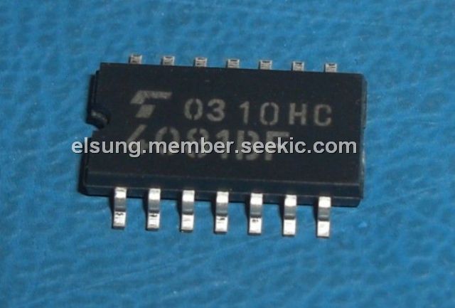
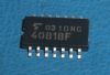
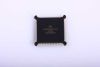
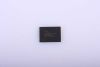
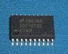
Product Summary
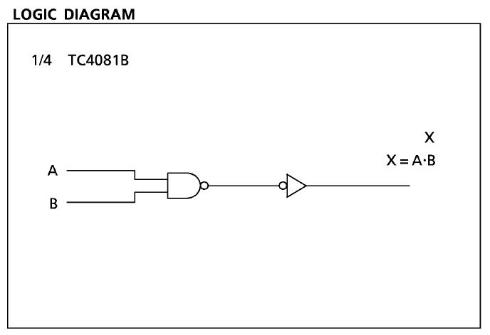
TC4081BF is a positive logic AND gate with two inputs respectively. Since all the outputs of TC4081BF are equipped with the buffer circuits of inverters, the input/output propagation characteristic has been improved and varistion of propagation time caused by increase of load capacity is kept minimum.
Parametrics
TC4081BF absolute maximum ratings: (1)DC supply voltage: VSS - 0.5~VSS + 20 V ; (2)Input voltage: VSS - 0.5~VDD + 0.5 V ; (3)Output voltage: VSS - 0.5~VDD + 0.5 V ; (4)DC input current: ±10 mA ; (5)Power dissipation: 300 (DIP)/180 (SOIC) mW ; (6)Operating temperature range: -40~85 ℃ ; (7)Storage temperature range: -65~150 ℃.
Features
TC4081BF electrical characteristics: (1)high-level output voltage: 4.95 V min; (2)low-level output voltage: 0.05 V max; (3)output high current: -0.61 mA min at VOH=4.6 V; (4)output low current: 0.61 mA min at VOL=0.4 V; (5)input high voltage: 3.5V min at VOUT=0.5V, 4.5V; (6)input low voltage: 1.5V max at VOUT=0.5V.
Diagrams
| Image | Part No | Mfg | Description |  |
Pricing (USD) |
Quantity | ||||
|---|---|---|---|---|---|---|---|---|---|---|
 |
 TC4081BF |
Other |
|
Data Sheet |
Negotiable |
|
||||
|
TC4081BFN |
Other |
|
Data Sheet |
Negotiable |
|
||||